


 (C:)
(C:) cs300
cs300
Computer
The cs600 covers the rudimentary elements of Computer Science and aims to enhance the work-related self-efficacy of someone only with a degree in Mathematics. This first post traces the arc from mechanical calculators to modern accelerators, covering the hardware that underpins all computation.
I
1.1. Computer
Babbage’s analytical engine (1837) is the first conceptual design of a general-purpose computer that separated a processing unit (i.e. the mill) from memory (i.e. the store), supported conditional branching and loops via three types of punch card, and was Turing-complete by modern definitions. Lovelace (1843) appended to her translation of Menabrea (1842) an algorithm computing Bernoulli numbers as the engine’s first program. A century later, Turing (1936) defined an abstract model of computation in which a finite control reads and writes symbols on an unbounded tape, so called the Turing machine, and proved that the Entscheidungsproblem (1928) is unsolvable.
Electronic switching produced the first electronic computers. The Electronic numerical integrator and computer (ENIAC, 1945), built by Eckert and Mauchly, is regarded as the first programmable, electronic, general-purpose digital computer. This equipped 17,468 vacuum tubes, occupied a 50×30-foot room, consumed ~150 kW, and performed up to 5,000 additions per second, orders of magnitude beyond electromechanical predecessors, though reprogramming it meant rewiring the machine by hand. Von Neumann (1945) described the stored-program concept, in which instructions reside in memory alongside data, so reprogramming means loading rather than rewiring.
The transistor, demonstrated in 1947 by Bell Labs (Nobel Prize in Physics, 1956), replaced vacuum tubes with smaller, faster, and more reliable devices that drew far less power. The next leap came with the integrated circuit (IC). Kilby at Texas Instruments built the first working IC on a germanium substrate in 1958 (Nobel Prize in Physics, 2000), while Noyce at Fairchild Semiconductor independently devised the planar silicon IC with aluminium metallisation in January 1959, which enabled mass production. The IC’s key innovation was consolidating transistors, resistors, and capacitors onto a single semiconductor substrate.
-
Five device generations, from vacuum tubes through transistors and ICs to VLSI.
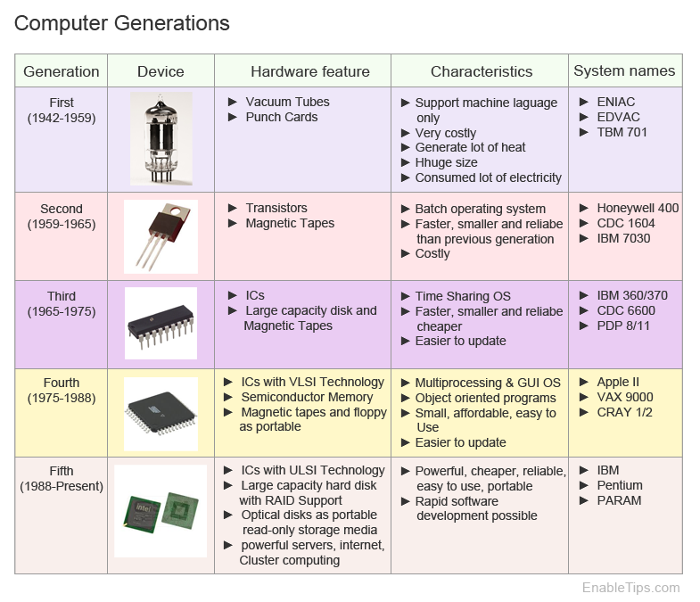
Moore’s Law drove successive waves of integration. Moore (1965) observed that the number of transistors per IC doubled every year (i.e. he revised to every two years in 1975), an empirical trend that guided the semiconductor roadmap for five decades. While packing more transistors would ordinarily raise power and heat, Dennard scaling (1974) held that as a transistor shrank, its voltage and current fell in step, so power per unit area stayed roughly constant. Moore’s rising count and Dennard’s constant power density together yielded clock speed (i.e. the rate the CPU steps, one cycle per tick, in Hz) and performance climb for the three decades within a fixed thermal budget.
The density continued to grow until an entire CPU fitted on a single chip. Specifically, the first commercial microprocessor arrived as the Intel 4004 (1971), commissioned by the Japanese calculator maker Busicom, and packed 2,300 transistors into a 4-bit CPU on a 12 mm² die. Such a single-core processor sits on a motherboard and reaches RAM, disk, I/O ports, and expansion slots (e.g. PCIe for a GPU) through buses and chipsets. This modularity permits each part to upgrade separately. The IBM PC (1981), built with this open architecture and Intel’s 8088 processor, then standardised personal computing and spawned the clone ecosystem that persists today.
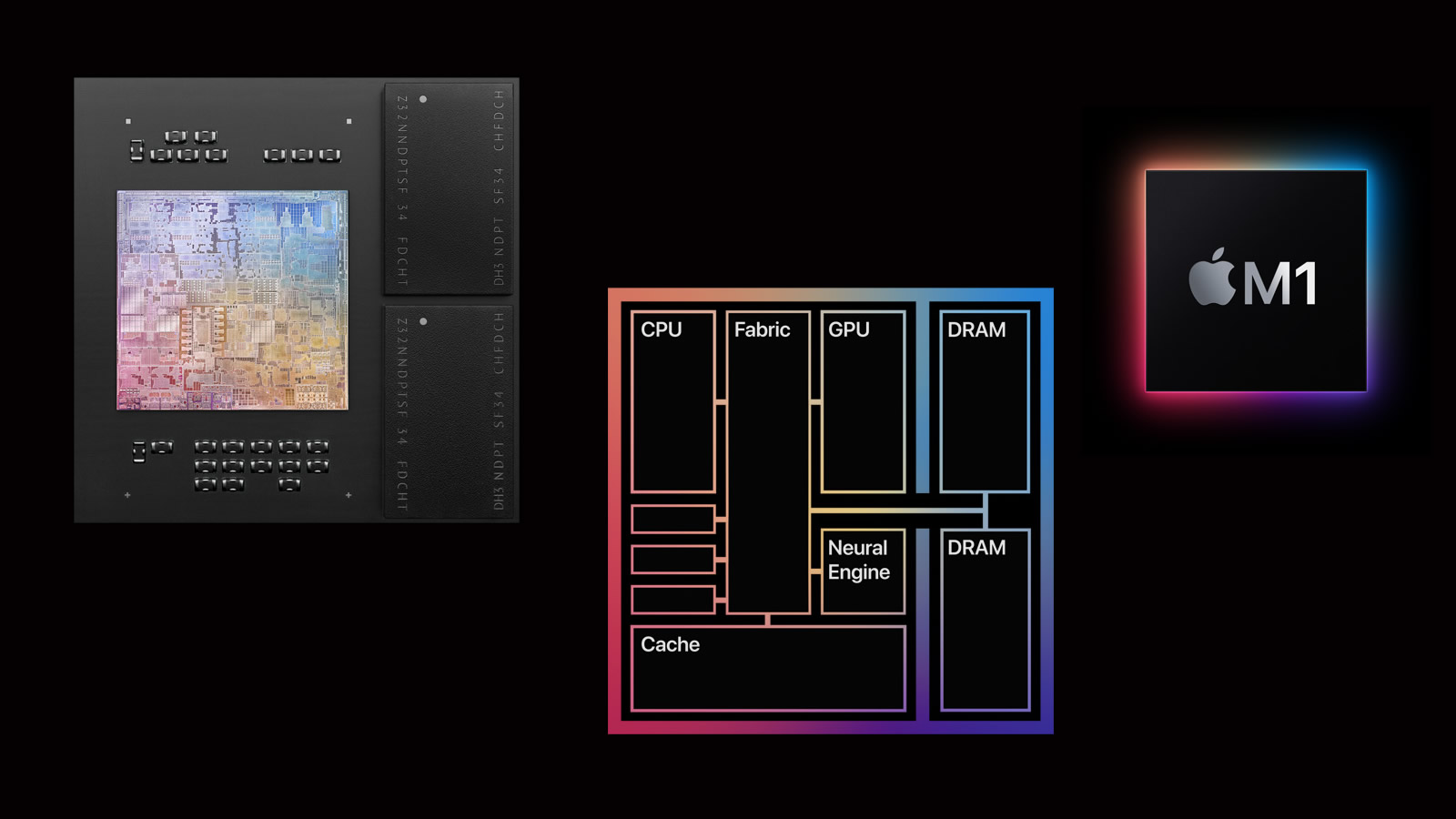
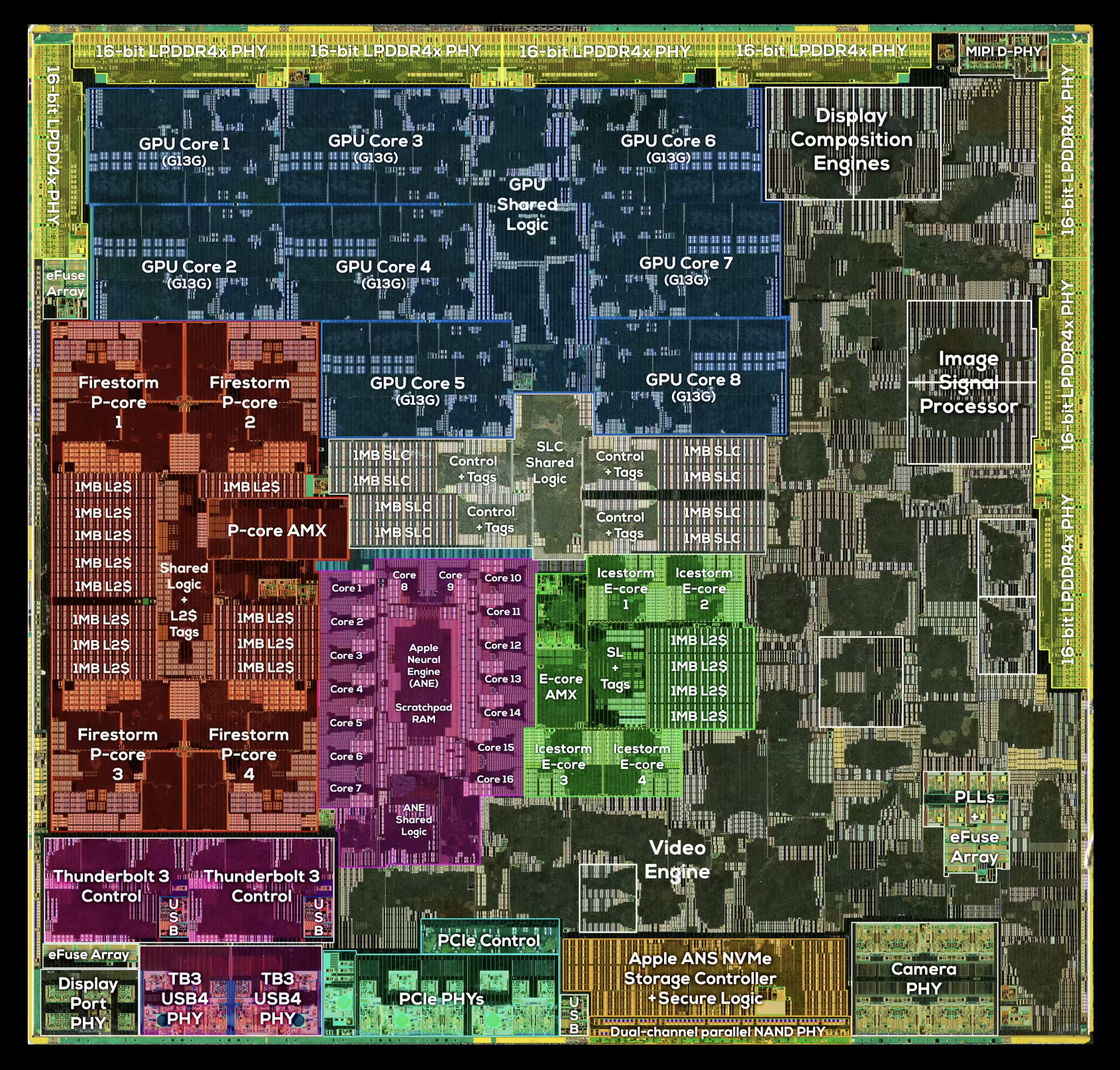
Dennard scaling finally failed around 2004 and clock speed plateaued at ~3-4 GHz, yet Moore’s count kept rising. The industry spent the transistors within the power budget, on more cores at lower frequencies (e.g. dual-core x86, 2005), and so on the system on chip (SoC). The SoC pulls the board’s essential components and special accelerators (e.g. NPU for ML inference) onto one die. For instance, Apple Silicon co-packages a 5 nm SoC of 16 billion transistors with LPDDR (i.e. a DRAM flavour alongside DDR, GDDR, and HBM) onto one substrate, and so built a system in package (SiP). Such integration is a matter of packaging and the memory model stays Von Neumann.
-
Two LPDDR packages flank the M1's SoC die, one DRAM pool shared by CPU, GPU, and Neural Engine.
-
The M1 die (2020), a single chip whose CPU cores stay Von Neumann.
1.2. Central Processing Unit
A central processing unit (CPU) implements an instruction set architecture (ISA), the software-facing interface specifying the supported operations, the registers they act on, and the addressing modes that name their operands. The microarchitecture is the implementation design of the interface (e.g. AMD’s Zen). It determines how the arithmetic logic unit (ALU), floating-point unit (FPU), and control unit (CU) cooperate. They differ in performance, yet a compiled binary executes unaltered on any CPU implementing the same ISA, as both Intel and AMD do for x86-64. Fabrication materialises the design in silicon, in-house (e.g. Intel) or at a foundry (e.g. TSMC, Samsung).
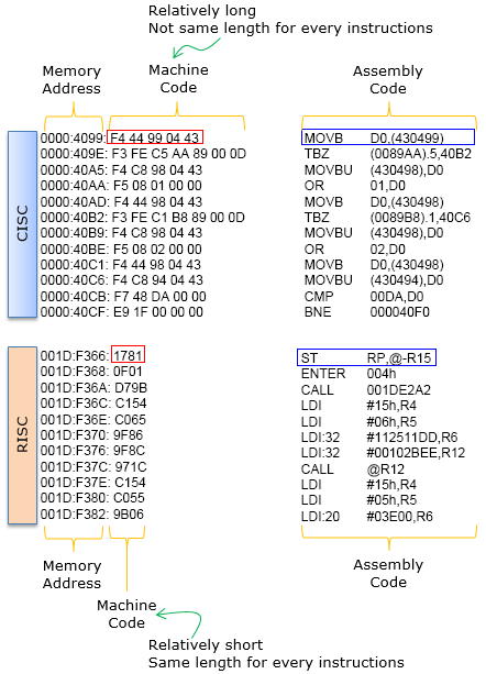
The two dominant ISA families reflect a fundamental trade-off between instruction density and simplicity. Intel’s x86 (1978) exemplifies complex instruction set computer (CISC), whose instructions vary in length, operate directly on memory, and admit diverse addressing modes. The set has grown past 1,500 instructions, almost none of which backwards compatibility permits removing, and the richness is billed to the microarchitecture. Variable length forces a bytewise scan for instruction boundaries, and hence x86 CPUs spend substantial die area on front-end decoders that crack instructions into fixed-width micro-ops ($\mu$ops), a RISC-like core behind a CISC interface.
Acorn RISC Machine (ARM, 1985) inverted the trade-off with reduced instruction set computer (RISC), whose ~350 instructions span a fixed 4 bytes, access memory only through explicit loads and stores, and retain operands in a large register file. Absent the bytewise scan, decode is simpler, pipelines shorter, and power per instruction lower. RISC does not remove the complexity but relocates it onto the compiler (§602#2.1), which schedules instructions and allocates registers such that several simple operations replace one CISC instruction. RISC-V (2010), royalty-free, advances the philosophy with a minimal base ISA (~47 instructions) and optional extensions.
-
One CISC multiply works directly on memory in five bytes, where RISC spells out load, multiply, store in fixed 4-byte instructions.
Given that an instruction pairs the opcode (i.e. the operation) and operands (i.e. the data it acts on), the CPU holds operands and control state in its on-chip registers, which include the program counter (PC), instruction register (IR), stack pointer (SP), and general-purpose registers (GPRs). At run time, the CPU loops a fetch-decode-execute cycle the stored-program model prescribes, i) fetch: the instruction at the PC enters the IR; ii) decode: the pair splits, the opcode to the CU and the operands to the ALU or FPU; iii) execute: the dispatched unit computes; and iv) write back: the result lands in a GPR before the PC steps. The machinery is indeed invariant across ISA families.
A CPU’s word size is its natural unit of data, the width of the ALU and data path in bits, which the GPRs match. The same $N$ bits also form a memory address so the CPU reaches at most $2^N$ bytes off-chip (e.g. $2^{32}$ = 4 GB). This memory is byte-addressable, its smallest unit one byte (i.e. 8 bits), yet neither its reach nor its granularity holds exactly in practice, since a design wires fewer address bits (e.g. x86-64 pairs 64-bit words with 48-bit virtual addr.) and the OS allocates in coarser 4 KB pages (§603#3.2). Addresses are written in hexadecimal (base-16, e.g. 0x7ffe), where each digit encodes 4 bits, and so a byte is two digits whose bits read off directly.
What the bits denote is fixed by convention. Unsigned integers read $N$ bits as base-2; two’s complement encodes a signed $-x$ as $2^N - x$, so a single adder serves both, with range $[-2^{N-1}, 2^{N-1}-1]$ and overflow modulo $2^N$ (§602#1.2). IEEE 754 (1985) splits a float into a sign, a biased exponent, and a mantissa, {1, 8, 23} bits for FP32, while BF16 retains the 8 exponent bits as {1, 8, 7} to trade precision for range. A multi-byte value occupies consecutive addresses, and endianness fixes their order; little-endian (x86, ARM) places the least significant byte first, a machine-local convention that serialisation must neutralise on the wire (§605#4.1).
-
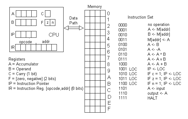
A minimal 4-bit CPU, the 16 opcodes on the right its entire ISA and the data path on the left its microarchitecture.
With the clock stalled at a few GHz, a faster chip can no longer come from a faster clock, and the iron law (Emer & Clark, 1984) shows what remains, factoring execution time as $\text{time} = \text{instructions} \times \text{CPI} \times \text{cycle time}$. Two of the three terms lie beyond the microarchitecture’s control. The instruction count is settled by the ISA and compiler, the stake CISC and RISC divide over, and the cycle time by the now-capped clock. That leaves cycles per instruction (CPI), the average cycles an instruction takes, as the one lever the microarchitecture can pull, and every technique that follows drives CPI down.
Pipelining overlaps the stages, so once it fills one instruction retires per cycle rather than one per $k$ cycles for a $k$-stage pipeline, and CPI approaches 1, while a superscalar core issues several per cycle across duplicated units to push it below 1. Out-of-order execution, first realised in Tomasulo’s algorithm (1967), keeps the pipeline fed by dispatching ready instructions regardless of program order. Register renaming makes this safe by mapping the ISA’s handful of architectural registers onto a larger physical file, so a reused name raises no false dependency, and reservation stations hold each instruction until its operands arrive.
Branch prediction guesses the direction of conditional branches (95-99% accuracy, 10-20 cycle penalty on misprediction), and speculative execution runs past the unresolved branch and discards the work on a wrong guess. That speculative state is architecturally invisible yet leaves microarchitectural traces in the cache, the side channel the Meltdown & Spectre (2018) vulnerabilities exploited. Such tricks extract instruction-level parallelism from one stream, but the returns diminish, which is why the clock plateau pushed the industry towards multiple cores and explicit parallelism (§604).
-
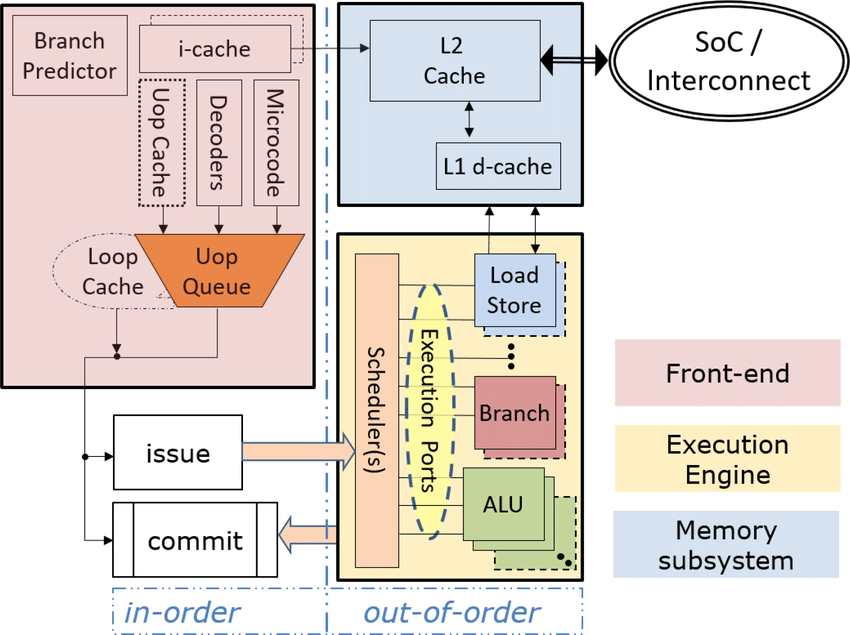
An abstracted core, the in-order front-end decoding into $\mu$ops that the out-of-order engine schedules across its ports.
1.3. Volatile Memory
Registers are fast but scarce (a few KB per core), so computer memory forms a hierarchy, where each level down accepts roughly an order of magnitude more latency in exchange for capacity at lower cost per byte. A cache hierarchy of L1 (~1 ns, 32-64 KB per core), L2 (~3-10 ns, 256 KB-2 MB), and L3 (~10-20 ns, tens of MB shared) is built from static RAM (SRAM), whose cell spends ~6 transistors per bit yet holds it as long as power lasts. L1 alone splits into separate instruction and data caches (a modified Harvard arrangement), while L2, L3, and main memory remain unified, so the model above the split stays Von Neumann.
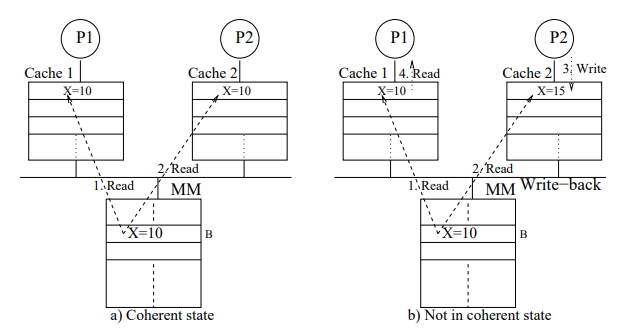
When multiple cores cache the same physical address, one core’s write can desync the others. Cache coherence protocols keep them aligned by invalidating stale copies. The MESI protocol assigns each cache line one of four states: {Modified, Exclusive, Shared, Invalid} and uses bus snooping or directory-based schemes to maintain coherence. False sharing occurs when unrelated data on the same cache line causes coherence traffic between cores. The overhead scales with core count, so coherence becomes a limiting factor in shared-memory parallelism (§604#2.2).
-
P2's write to X leaves P1's cached copy stale, the incoherence that MESI exists to prevent.
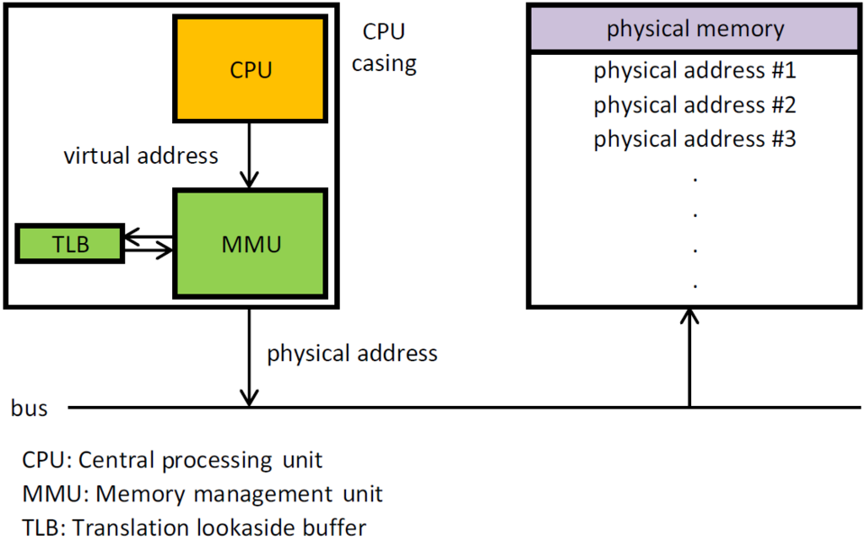
Virtual memory interposes a translation layer between the addresses a program issues and physical RAM, so each program names a large, contiguous space of its own without regard to where its data physically resides. Both the virtual space and physical RAM divide into fixed-size pages and frames (typically 4 KB), and every virtual address splits into a page number and an offset, of which only the page number is translated. The memory management unit (MMU) maps each virtual page to a physical frame through a per-process page table, then concatenates the untouched offset to form the physical address. Because that table itself resides in memory, the translation lookaside buffer (TLB), a small SRAM cache of recent mappings, answers the common case in one or two cycles, so most accesses bypass the table entirely.
A TLB miss sends the MMU to walk the page table in hardware, four dependent memory reads on x86-64’s four-level structure, after which it caches the mapping for reuse. The cost of a single reference thus spans orders of magnitude, roughly one cycle on a TLB hit, a few hundred on a walk, and millions on a page fault. A page fault arises when translation cannot complete, most commonly because the page resides on disk rather than in a physical frame, whereupon the CPU traps to the OS kernel, which fetches the page and restarts the instruction. Everything up to the trap is hardware mechanism, whereas which frame to evict, how to isolate processes, and whether to overcommit are policy the OS sets (§603#3.2).
-
The MMU translates virtual to physical on the way to the bus, the TLB answering the common case.
Off-chip main memory uses dynamic RAM (DRAM), which stores each bit in a single transistor plus capacitor, far denser and cheaper but slower (~50-100 ns), and dynamic because the capacitor leaks, so every bit must be refreshed every ~64 ms. Data moves between levels in cache lines (typically 64 bytes), and a well-designed program achieves high temporal and spatial locality, i.e. it re-references an address within a short window and references addresses within one cache line, to minimise cache misses that cascade through successively slower levels.
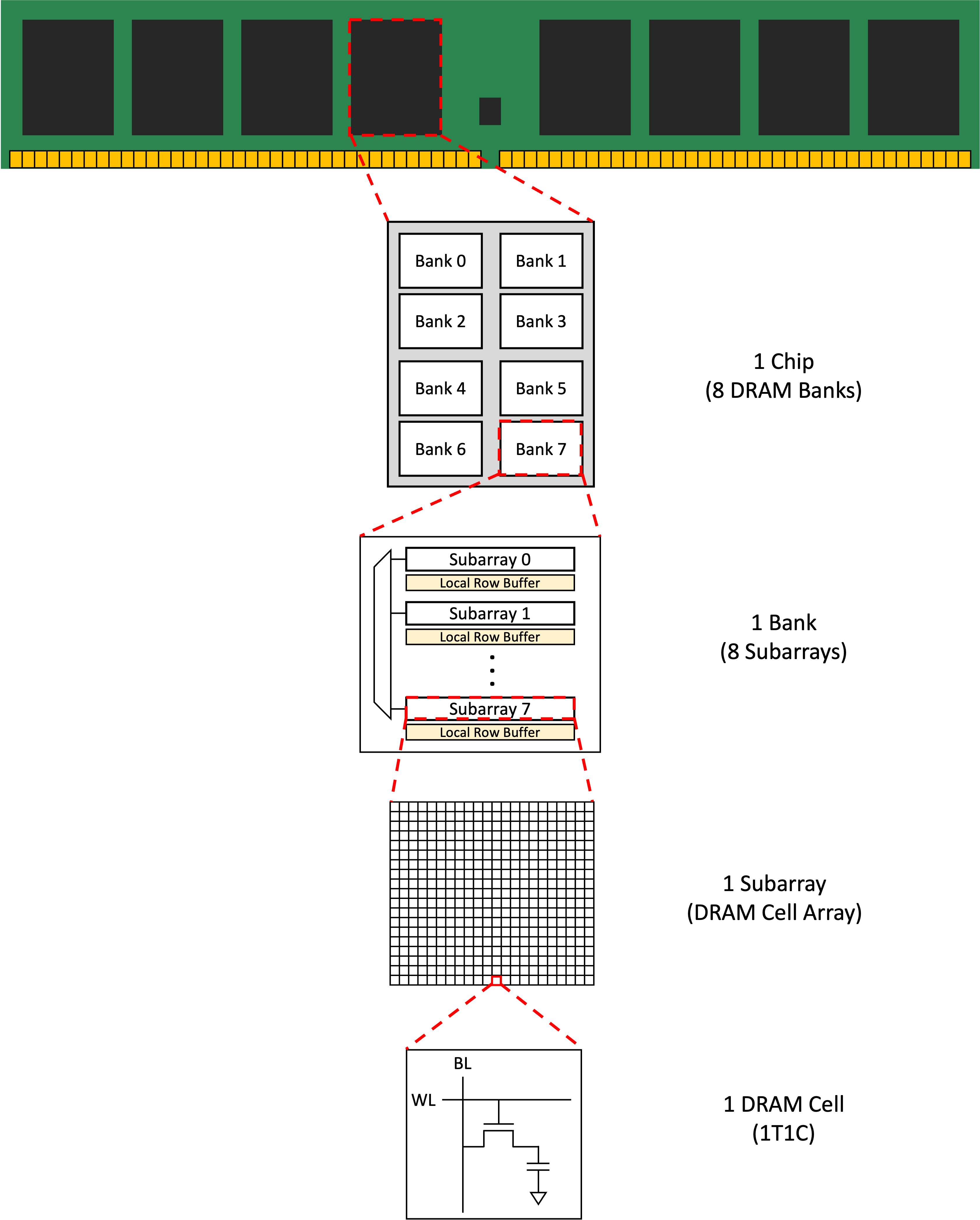
DRAM packs its density into banks, each a grid of rows and columns of 1T1C cells. Reaching a byte first activates its entire row into a row buffer (the row access, RAS), then selects one column from it (the column access, CAS). A later access to the same row, a row hit, reads straight from the buffer and is fast; a different row, a row conflict, must precharge and re-activate at far higher cost. Spatial locality therefore pays twice, a cache-line fill above and a row-buffer hit below, so sequential access outruns random at every level of the hierarchy. Scanning a row-major matrix with its contiguous index innermost (for i: for j: A[i][j]) runs several times faster than the swapped order, which strides a full row per step and misses in both the cache and the row buffer. Volatile throughout, both SRAM and DRAM forget on power loss; what survives the cut is persistent storage.
-
One DIMM unpacked, chip to bank to subarray down to the 1T1C cell.
1.4. Persistent Storage
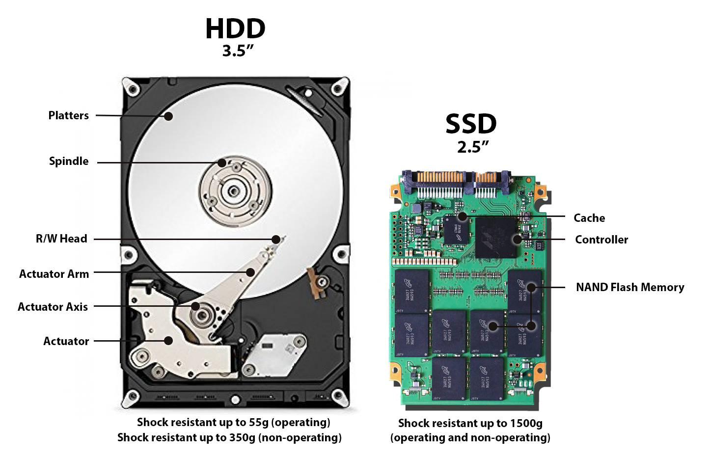
Persistent storage retains data without power supply. Specifically, hard disk drives (HDDs) store data magnetically on spinning platters with read/write heads on an actuator arm. Performance is dominated by mechanical delays: seek time (~10 ms average) for the head to reach the correct track, and rotational latency (half the rotation period, ~4.2 ms at 7,200 RPM) for the platter to bring the desired sector round under the head. Sequential throughput reaches 100-200 MB/s, but random access is severely limited by the physical movements. Driven by falling NAND prices and Intel’s early consumer drives, SSDs had largely replaced HDDs for primary storage by the late 2010s.
Solid-state drives (SSDs) use NAND flash memory, where each cell is a transistor with an electrically isolated floating gate, and the cells are organised into pages (~4-16 KB, the unit of read/write) and blocks (256-512 pages, the unit of erase). This asymmetry, where data is programmed at page level but erased at block level, necessitates its own garbage collection (relocating valid pages from partially-stale blocks, then erasing them, Ref) and the TRIM command (letting the OS notify the SSD when files are deleted). Each cell has a limited number of program/erase cycles (1K-100K, fewer as more bits are packed per cell), so wear leveling distributes writes evenly across the device.
The flash translation layer (FTL), firmware inside the drive, is what hides this management, maintaining a mapping from logical block addresses to physical pages so that garbage collection and wear leveling proceed behind an unchanged block interface. Performance follows from the absence of mechanics, as a NAND read costs ~25-100 μs against the HDD’s ~10 ms, sequential throughput reaches several GB/s, and random I/O climbs from the HDD’s ~100-200 IOPS to hundreds of thousands. The interface lagged the medium, as SATA/AHCI, designed for disks around one shallow command queue, caps throughput near 550 MB/s, so NVMe (2011) attaches flash directly to PCIe with up to 64K queues of 64K commands each, and modern drives deliver 7-14 GB/s with over a million IOPS.
-
The HDD's platters and actuator against the SSD's controller and NAND packages.
Read end to end, the hierarchy obeys a single constraint, that the throughput of the whole is bounded by the slowest link an access must traverse, the Von Neumann bottleneck in its general form. The bound tightens with time, since processor speed historically outgrew DRAM latency, a divergence Wulf and McKee (1995) named the memory wall. Each boundary therefore earns a cache of its own, SRAM before DRAM, the row buffer before the cell array, the DRAM and SLC caches before NAND, and AMD’s 3D V-Cache spends an entire stacked die on nothing but extra L3. When main memory overflows, the OS pages to storage and the hierarchy degenerates, every reference now risking the millisecond cost of its slowest member (§603#3.2). The accelerators ahead inherit both walls at once, answering the stalled clock with parallelism in the thousands of lanes and the memory wall with ever wider links, so their design is largely the problem of feeding arithmetic faster than data can move.
II
2.1. Graphics Processing Unit
A graphics processing unit (GPU) answers the stalled clock by spending its transistors in the opposite direction to the CPU, which devotes most of its die to making one thread fast via caches, branch prediction, and out-of-order machinery. The GPU instead packs thousands of arithmetic units and lets each thread run slowly. Flynn’s taxonomy classifies designs by instruction and data streams, wherein a single core is SISD, a multi-core CPU MIMD, and SIMD vector units (e.g. AVX) apply one instruction to many elements. The GPU extends this to SIMT (single instruction, multiple threads), groups of threads executing the same instruction in lockstep on different data.
Early GPUs were fixed-function hardware for graphics rendering, hardwiring vertex transformation, lighting, rasterisation, and texturing with no programmability. NVIDIA’s GeForce 256 (1999), marketed as the world’s first GPU, moved hardware transform and lighting onto the graphics card but kept the pipeline fixed. Programmable shaders arrived with the GeForce 3 (2001), and the decisive shift came with the Tesla microarchitecture (2006) whose GeForce 8800 GTX was the first GPU with unified shaders, merging vertex and pixel processors into general-purpose streaming processors so that no fixed-function stage sat idle when another was saturated.
Compute unified device architecture (CUDA), released in 2007, made GPUs programmable for general-purpose computing by providing a C-based programming model that abstracted away graphics concepts. Before it, general-purpose GPU computing required abusing graphics APIs, which expressed computations as texture operations in OpenGL shading language (GLSL) or C for graphics (Cg). Matrix operations exhibit data parallelism that maps naturally onto GPU hardware, and CUDA’s ecosystem would later prove decisive for the deep learning revolution (§602#2.2 examines its compiler).
A discrete GPU (dGPU) sits on a separate PCIe card with its own dedicated VRAM (e.g. NVIDIA A100, 80 GB HBM2e), while an integrated GPU (iGPU) shares the die and main memory with the CPU (e.g. Apple Silicon). iGPUs are power-efficient but lack the memory bandwidth and compute density of discrete cards. ML frameworks (PyTorch, JAX) abstract the hardware behind device backend APIs, e.g. torch.device(“cuda | mps | cpu”), dispatching kernels and memory allocation to the appropriate driver. CUDA’s mature toolchain (cuDNN, cuBLAS, NCCL, TensorRT) gives NVIDIA a dominant position in production ML.
-
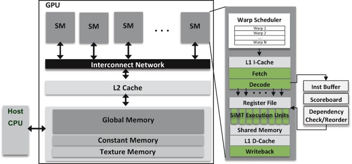
SMs over one interconnect to a shared L2 and device memory, each SM with its own scheduler and register file.
GPU compute performance is measured in floating-point operations per second (FLOPS). Peak FLOPS depends on core count, clock speed, and precision format, with lower precision yielding higher throughput since more operations fit per cycle. For instance, the A100 delivers 19.5 TFLOPS at FP32 and 312 TFLOPS at FP16 via tensor cores, while achieved FLOPS falls well below peak in practice due to memory stalls, warp divergence, low occupancy, and synchronisation overhead. Hence, Model FLOPS utilisation (MFU), which is the ratio of achieved to theoretical peak, is the standard efficiency metric for training runs, where 30-60% is typical at scale.
Notice that FLOPS and FLOPs, distinguished only by the case of the final letter, measure different things. FLOPS is a rate, counting floating-point operations completed per second, used in peak-performance claims as in “312 TFLOPS on the A100”. FLoating point OPerations (FLOPs) is a count measuring the total operations in a workload, used in ratios like arithmetic intensity (FLOPs/byte) or training budgets ($\sim 3.14 \times 10^{23}$ FLOPs for GPT-3). The two relate via “wallclock time” $\approx$ “total FLOPs” $/$ “effective FLOPS”, so the same workload runs faster either by reducing its FLOPs (e.g. quantisation, sparsity) or by raising delivered FLOPS (e.g. better kernels, higher MFU).
2.2. Streaming Multiprocessor
A GPU consists of streaming multiprocessors (SMs), each a self-contained processing unit with its own register file, shared memory/L1 cache, warp schedulers, and execution units. The fundamental scheduling unit is a warp, a bundle of 32 threads executing the same instruction in lockstep, following the SIMT model. If threads within a warp take different branches (warp divergence), the SM executes each path separately and wastes slots for inactive threads. Each SM runs multiple warp schedulers that switch to a ready warp the moment one stalls on a memory access, hiding memory latency through parallelism (i.e. more threads) rather than large caches.
That hiding works only while another warp stands ready, and occupancy measures the supply, the ratio of warps resident on an SM to the hardware maximum (64 on recent architectures). A global-memory access stalls a warp for hundreds of cycles, so the schedulers need tens of residents to always find an eligible instruction. Residency in turn draws on the SM’s fixed budget of registers and shared memory, of which every thread claims a share, so a kernel that spends too many registers per thread leaves warp slots unfilled and the stalls exposed. Much of the MFU shortfall originates here, as low occupancy starves the tensor cores however fast they multiply.
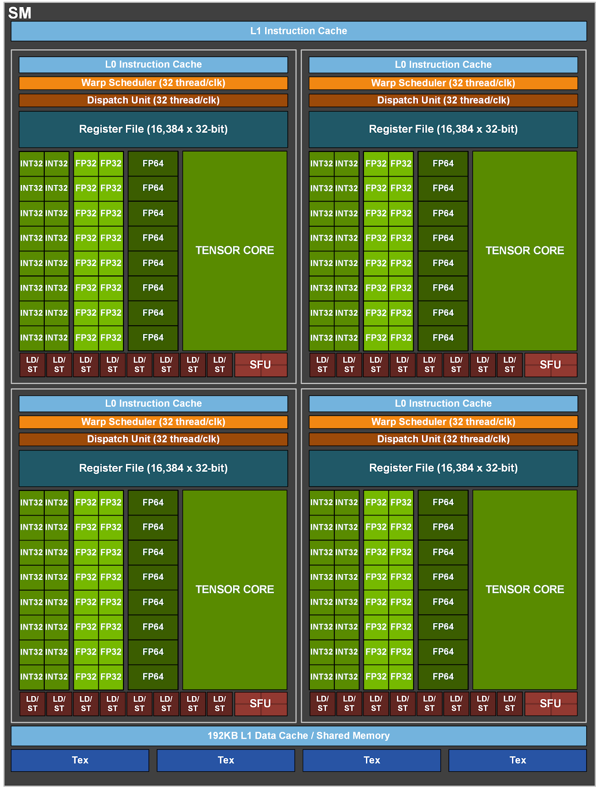
A CUDA core is a scalar execution unit within an SM that performs one fused multiply-add (i.e. two FLOPs) or integer operation per cycle per thread. They suit graphics and general parallel workloads but lack hardware for the dense matrix multiply-accumulates (MMAs), which together with non-linear activation functions are the heart of deep learning. Tensor cores, introduced with Volta in the V100 (2017), address this by performing a 4×4×4 mixed-precision matrix multiply-accumulate (FP16 × FP16 → FP32), i.e. 64 multiply-adds per clock. The V100’s 640 tensor cores deliver 125 TFLOPS mixed-precision, an order of magnitude beyond its 15.7 TFLOPS FP32 CUDA throughput.
Micikevicius et al. (2017) showed that most forward and backward computations tolerate FP16 precision, with only weight updates requiring FP32 accuracy. Two techniques make this work, i) maintaining an FP32 master copy of the weights; and ii) loss scaling to preserve small gradients in FP16’s limited range. PyTorch packages the recipe as automatic mixed precision (AMP) via torch.cuda.amp. Subsequent generations expanded tensor core support, as the Ampere architecture in the A100 (2020) added TF32, BF16, and structured sparsity (2:4 pattern, up to 2× speedup).
The Hopper architecture in the H100 (2022) introduced the Transformer Engine, hardware-software logic that dynamically chooses between FP8 and FP16/BF16 precision per layer during training. The Blackwell architecture in the B200 (2024) followed with a 2nd-generation Transformer Engine. GPU hardware thus co-evolved with the transformer’s scaling. Tensor cores shifted towards transformer workloads through lower-precision formats (FP8, FP4) and on-chip precision management, while attention speedups come from software exploiting new memory engines (e.g. Hopper’s asynchronous tensor memory accelerator) rather than any native attention primitive.
-
An Ampere SM, each quadrant pairing INT32/FP32/FP64 lanes with a tensor core.
2.3. Device Memory
GPU memory forms a deep hierarchy of its own, where each SM has a register file (~256 KB on Volta) and shared memory / L1 SRAM (48-164 KB), all SMs share an L2 cache (40 MB on the A100), and off-chip global memory (HBM/GDDR) holds the most capacity at 200-600 cycle latency. Software masks the transfer at the widest boundary, between host and device. Direct memory access (DMA) lets the GPU read/write host memory without CPU involvement, but the DMA engine operates on physical addresses and cannot safely access pageable host memory since the OS may swap it out. The CUDA driver therefore stages data via a page-locked (pinned) buffer before initiating DMA.
High-bandwidth memory (HBM), the flavour of VRAM on AI accelerators, achieves its performance through vertical stacking, where multiple DRAM dies are interconnected by through-silicon vias (TSVs) and mounted on a silicon interposer next to the GPU die. Each stack exposes a 1,024-bit interface at moderate clock speeds, opposite to GDDR’s narrow buses at high clock speeds. Successive generations from SK Hynix and Samsung pushed per-stack bandwidth from ~250 GB/s (HBM2) to ~1.2 TB/s (HBM3e), and the H100’s five HBM3 stacks deliver 3.35 TB/s for 80 GB. Wider bus and lower power per bit make HBM the AI/HPC standard.
-
HBM dies stacked over TSVs beside the processor on a silicon interposer.

The roofline model in Williams et al. (2009) formalises attainable performance as $P = \min(P_{\text{peak}},\ I \times BW)$, where a kernel’s arithmetic intensity $I$ (FLOPs/byte moved from memory) places it under either the flat ceiling of peak FLOPS (compute-bound) or the sloped bandwidth ceiling (memory-bound), the two meeting at the ridge $I^* = P_{\text{peak}}/BW$. Intensity is the kernel’s own property, as a matmul performs $O(n^3)$ FLOPs on $O(n^2)$ bytes and its intensity grows as $\sim n$, crossing the ridge with size, whereas an elementwise operation stays at $O(1)$, pinned to the bandwidth slope. Modern GPUs push the ridge outward, with an H100 needing $989/3.35 \approx 300$ FLOPs/byte to saturate BF16 tensor cores, far above what most kernels reach.
In their unfused implementations, attention $\mathrm{softmax}(QK^\top)V$, embeddings $E[i]$, and activations $\sigma(x_i)$ are memory-bound, while large matmuls $C = AB$ are compute-bound. Every unfused operation also pays a full HBM round-trip, writing its output tensor only for the next to read it back, so compilers fuse chains of them into one kernel whose intermediates stay in registers (§602#3.2). Dao et al. (2022) carried the idea to attention with FlashAttention, which tiles $Q$/$K$/$V$ into shared memory blocks and fuses softmax’s row-wise normalisation into the tiled matmul, so the $N \times N$ score matrix never materialises in HBM, converting a memory-bound operation into a compute-bound one.
-
Tiling Q, K, V through SRAM so the $N \times N$ score matrix never lands in HBM.

What fills the memory decides how the device is bought. Training holds the weights, their gradients, and the optimiser’s moments, roughly 16 bytes per parameter under mixed-precision Adam before activations claim their share, so capacity bounds the largest model a single card trains. Inference inverts the constraint, as decoding each token streams every weight past the arithmetic for a handful of FLOPs per byte, an intensity far below the ridge, so serving throughput tracks bandwidth instead. The two datasheet numbers that matter hence precede any FLOPS figure, capacity for training and bandwidth for serving.
2.4. Interconnect
PCIe is the standard system interconnect, roughly doubling bandwidth per generation (Gen), from ~4 GB/s ×16 (Gen 1, 2003) to ~128 GB/s (Gen 6, 2022, via PAM-4 modulation). A PCIe link aggregates full-duplex serial lanes (×1, ×4, ×8, ×16) with differential signalling, replacing the shared parallel PCI and AGP buses of the early 2000s. Yet for multi-GPU HPC and AI workloads this is insufficient, as training large models exchanges gradients and activations at rates that saturate even Gen 5.
NVLink (Pascal) is a GPU-to-GPU interconnect, also doubling per generation, from 160 GB/s (1.0, P100) to 1.8 TB/s (5.0, B200). NVSwitch (Volta) is a switch chip giving all-to-all GPU links at full NVLink bandwidth, past point-to-point topology limits. DGX systems pack these into multi-GPU servers (e.g. DGX H100 with 8× H100), while the GB200 NVL72 wires 72 Blackwell GPUs at 1.8 TB/s into a rack-scale node. The nvidia collective communications library (NCCL) implements topology-aware all-reduce, all-gather, and broadcast primitives, the backbone of distributed training in PyTorch and JAX.
For cluster-level communication, InfiniBand, a switched fabric for HPC and AI clusters, provides remote DMA (RDMA), enabling zero-copy transfer at sub-$\mu\mathrm{s}$ latency by bypassing the kernel socket path that ordinary network I/O traverses (§605#2.2). Bandwidth has grown from SDR (10 Gbps) to NDR (400 Gbps) and XDR (800 Gbps), and NVIDIA acquired Mellanox (2020) to own the fabric its clusters ride on. The emerging Compute Express Link (CXL) standard, on the PCIe physical layer, adds cache-coherent protocols (CXL.io, CXL.cache, CXL.mem) letting CPUs and accelerators share coherent memory, unlocking heterogeneous compute and memory pooling.
-
The card's edges, PCIe to the motherboard and an interconnect interface, around the GPU and its VRAM.
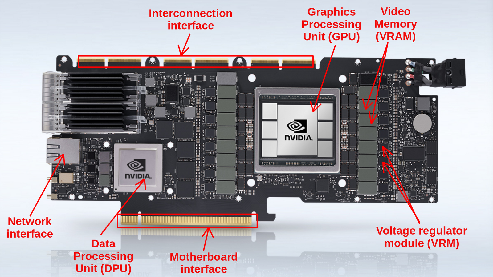
The links assemble into a bandwidth hierarchy that mirrors the memory one, HBM on the package (TB/s), NVLink within the node (hundreds of GB/s), and PCIe or InfiniBand between nodes (tens), each boundary shedding roughly an order of magnitude. A collective operation is billed at the slowest link it crosses, so distributed training partitions the model and the batch to keep the heaviest exchanges on the fastest tier (§608). The whole machine, read end to end, thus remains bounded by data movement rather than arithmetic.
–>
 me.bat
I gathered words solely for my own purposes without any intention to break the rigour of the subjects.
I also prefer eating corn in spiral .